

A Modern Chip Is Built Twice
Before a modern chip reaches a factory, engineers have already built and tested a detailed digital version of it.
Many chip companies are fabless: they design chips but outsource production to a foundry, a specialist factory that manufactures designs for others. Companies such as Intel and Samsung also operate as integrated device manufacturers, designing and producing their own chips while offering manufacturing services to external customers.
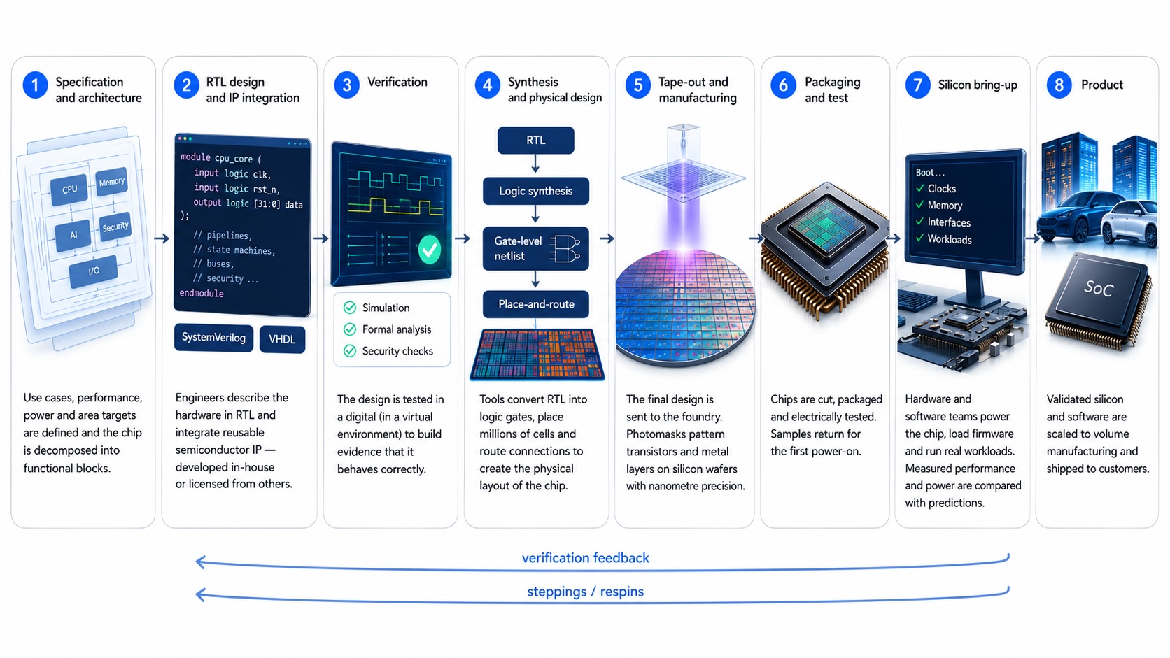
By the time fabrication starts, the design is a complete set of instructions defining how the chip works and how it is physically built. Because errors become much more expensive after this point, most problems must be found before the first wafer is processed.
The first build takes shape step by step
A chip does not appear as one perfect digital copy from the beginning. It is developed through a series of increasingly detailed models, much like a building moves from an initial concept to architectural plans, engineering drawings and finally construction instructions.
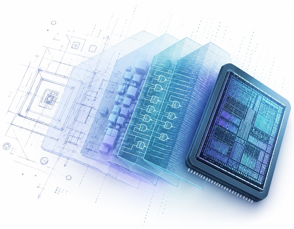
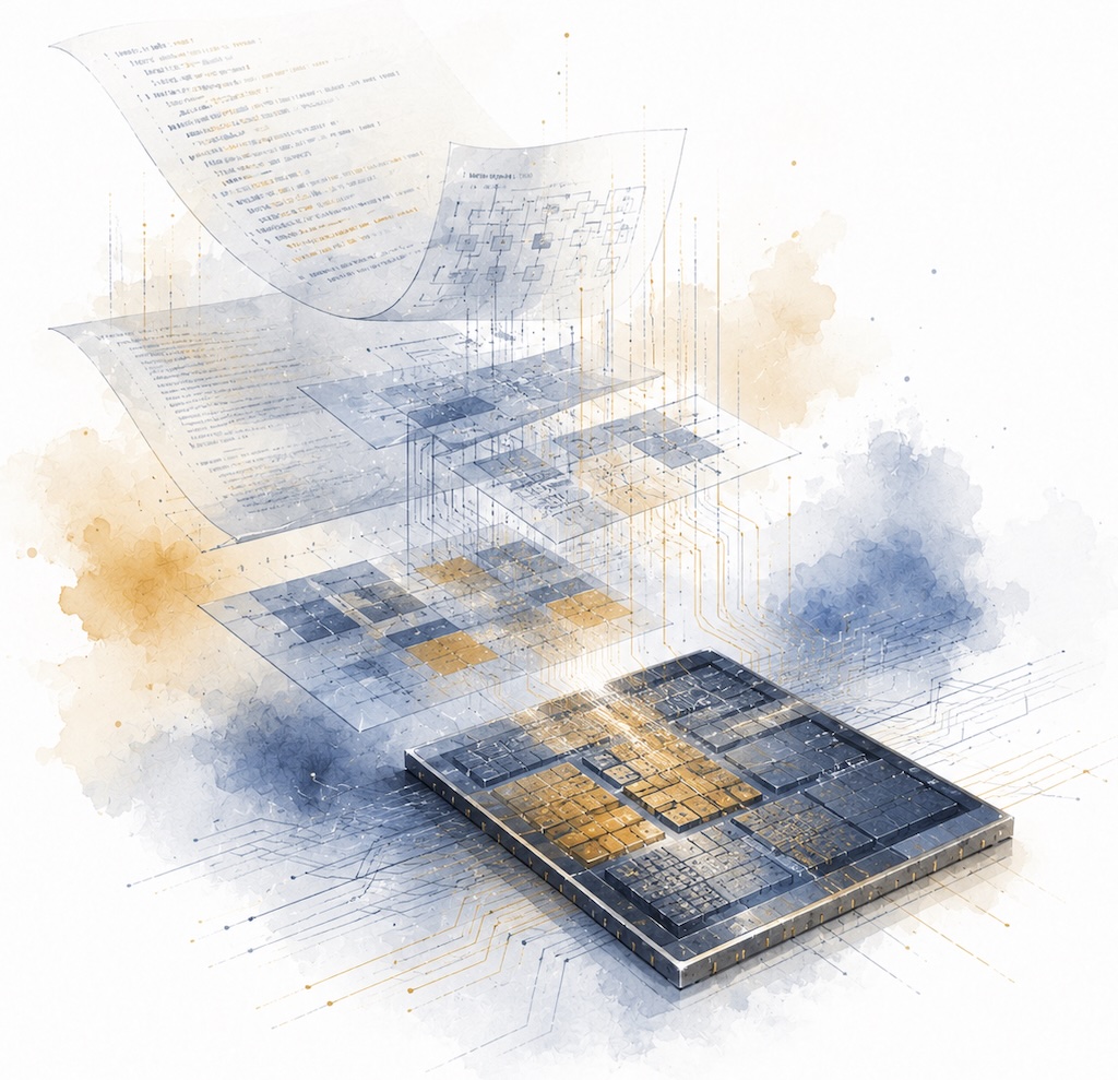
Early functional models test whether the proposed chip can deliver the envisioned features, while targeted modeling gives insights into performance and power efficiency. The system architecture defines its main building blocks and how they communicate. Register-Transfer Level (RTL) language then describes exactly how the digital logic should behave from one clock cycle to the next.
Later, automated tools translate that behaviour into logic gates and determine the physical position of every circuit element and connection. The final result is a manufacturing database containing the precise geometric patterns that the foundry will reproduce on the wafer.
Architecture sets the PPA budget
The process starts with workloads and measurable targets. Architects decide how much computing power is needed, how data moves through memory, which functions should be implemented in hardware, and how the chip should be divided into subsystems such as processor cores, AI accelerators, security engines, memory blocks and controllers, external communication interfaces, internal data connections, and clock and power-management circuits.
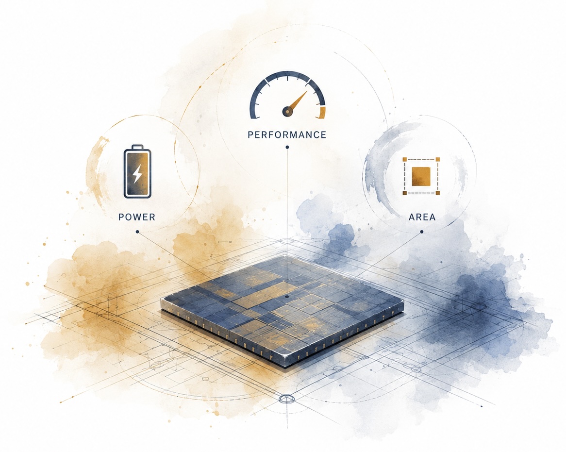
PPA means Performance, Power and Area. Performance describes how much useful work the chip can complete within a given time while meeting the needs of its intended applications. Power includes active consumption, leakage and energy used per task. Area determines the die size - the physical size of each chip cut from the wafer - which strongly affects manufacturing cost and yield, the percentage of manufactured dies that pass testing and can be sold.
These targets compete with one another. Improving performance may require more circuitry or higher power. Reducing power can limit speed, while a smaller die may improve cost and yield but leave less space for memory or accelerators. Chip design is therefore a search for the best balance rather than the maximum of any single metric.
At this stage, PPA comes from Python, C++ or system-level models. The estimates are approximate, but they can reveal a memory or compute bottleneck, an accelerator that is too large or a power budget that cannot be met before detailed design begins.
RTL and HLS create the functional chip
Engineers describe hardware mainly in languages such as SystemVerilog or VHDL. RTL defines pipelines, state machines, buses, memory controllers and security logic, including what changes on every clock cycle. For some algorithmic blocks, High-Level Synthesis (HLS), can instead translate descriptions written in languages such as C++ or SystemC into RTL. HLS can accelerate development, but engineers must still define timing, parallelism and hardware constraints carefully.
A modern chip is usually assembled from reusable functional blocks known as semiconductor IP, or IP cores. These may include processor cores, memory controllers, communication interfaces, security engines or AI accelerators. Some are developed in-house, while others are licensed from specialist suppliers. Much of chip design therefore consists of selecting, adapting and connecting proven blocks so that they work together correctly.
AI tools can support this stage by generating and reviewing RTL, translating higher-level descriptions into hardware structures, proposing alternative implementations and optimising logic for performance, power or area. They can also assist with test generation, formal properties, documentation and analysis of large codebases, helping engineers explore more design options in less time.
Test chips answer questions models cannot
Some technologies depend too strongly on real transistor behaviour and manufacturing variation to be validated only in software. Before committing them to a full SoC (System-on-Chip), engineers may fabricate a test chip: a small, purpose-built piece of silicon containing only the new circuit or technology that needs to be verified.
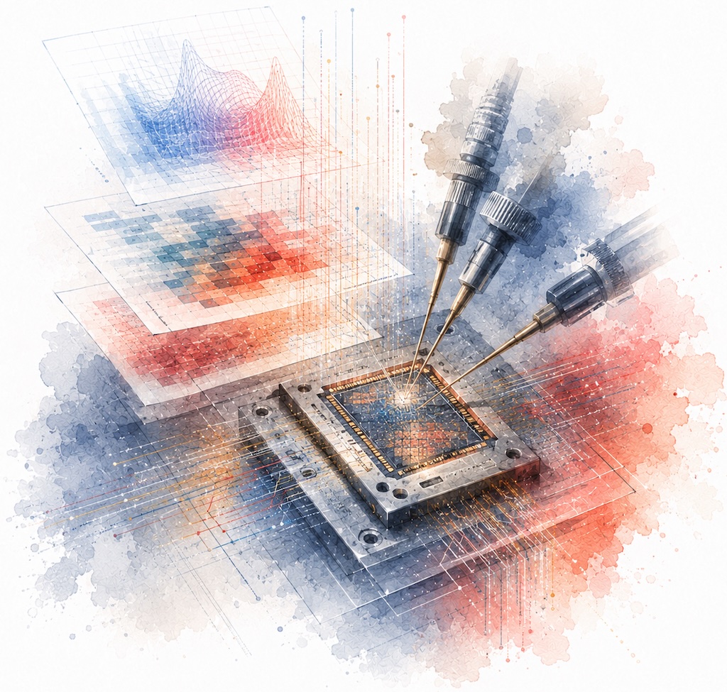
A Field-Programmable Gate Array (FPGA), can imitate digital logic and run early software, but it cannot reproduce the final chip’s transistor characteristics, wire delays, analog effects, leakage or physical size. A test chip provides real measurements from manufactured silicon. Engineers use those results to refine circuit models, operating margins, test methods and integration rules before placing the technology inside a more complex and more expensive chip.
Such test chips are often used for new memories, analog circuits, high-speed interfaces, PHYs (the physical circuits that transmit and receive signals) or Physically Unclonable Functions (PUFs) used to create a unique hardware identity.
Synthesis and physical design create digital silicon
A process called logic synthesis converts the RTL description into a gate-level netlist - a detailed list of logic gates, registers and their connections. These elements are selected from a library supplied or approved by the foundry for the chosen manufacturing process. The synthesis tools, stochastic by nature and design, try different implementations to meet targets for clock speed, power consumption and chip area while preserving the behaviour defined in the RTL.

The netlist is then transformed into the physical layout of the chip. Engineers divide the die into regions for processors, memories and accelerators, build the power-distribution and clock networks, place millions of standard cells and route their connections across multiple metal layers. At each step, specialised tools check whether signals arrive within the required time, power reaches all parts of the chip reliably, nearby wires interfere with one another, and the layout follows the foundry’s manufacturing rules.
By the end of physical design, every cell has a location and every connection has a route. The chip still exists only as digital data, but that data now describes the exact structure the foundry can manufacture.
PPA is recalculated at every stage
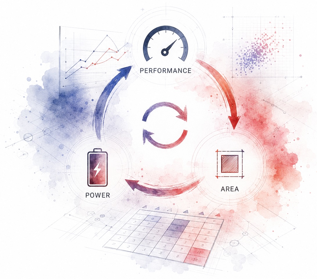
Performance, power and area are not measured only once. Architectural models estimate how the chip will handle its target workloads. RTL simulation measures clock cycles and data movement. Synthesis estimates gate count, timing and power. Place-and-route adds the effects of real wire lengths, routing congestion and final layout area. The completed layout is then checked under different manufacturing variations, supply voltages and operating temperatures before it is released for production.
The three targets interact. Higher frequency may require larger cells and more buffers, increasing power and area. More memory may improve performance but enlarge the die. Lower voltage saves energy but reduces timing margin. Physical implementation therefore often sends the design back to architecture or RTL for another iteration.
Tape-out starts the second build
Before manufacturing, the completed layout goes through a final set of checks known as sign-off. Engineers confirm that signals arrive on time, the geometry follows the foundry’s rules, the physical layout matches the intended circuit, power can be delivered safely and the chip can be tested after fabrication. Once these checks pass, the digital design is considered ready to manufacture.

The next milestone is tape-out: the final manufacturing database is released to the foundry. The foundry uses it to create photomasks, which act like highly precise templates for building the chip layer by layer on a silicon wafer. Materials are deposited, patterned with light, implanted and etched repeatedly to form the transistors and the metal connections above them.
The factory does not decide how the circuit should work. It reproduces, with extreme precision, the structure already defined in the digital design.
First silicon shows whether the digital model matches reality
When the first chips return, engineers begin silicon bring-up: powering the device, checking clocks, resets, memories and interfaces, then loading firmware and running test workloads.
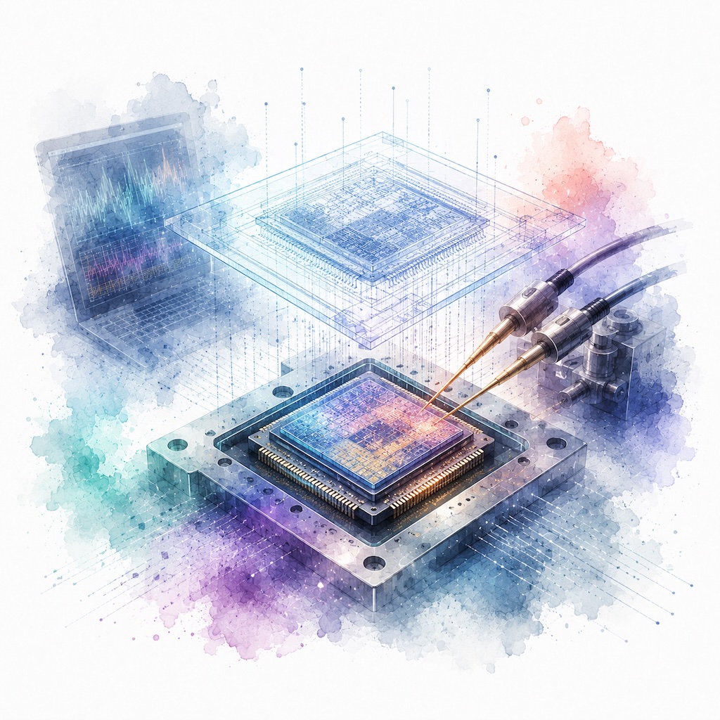
The software must already be ready. Boot code, drivers and diagnostic tools are developed alongside the chip using simulations and FPGA prototypes. Without them, engineers cannot properly test the hardware.
They then compare measured speed, latency, power, leakage and temperature with earlier predictions. Yield data shows how many chips work correctly and whether production is economical.
A chip may function correctly but still be too slow, power-hungry, hot or unreliable under real operating conditions. Bring-up therefore validates the complete hardware-software platform, not just the silicon.
One product may require several silicon steppings
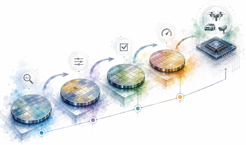
The first manufactured version of a chip is often labelled A0. A stepping is a revision of one or more photomasks used to fabricate the chip. Early steppings support bring-up, characterisation and defect discovery; corrected versions may follow as A1 or A2, while a broader redesign may receive a new letter, such as B0, and later become the production version. In many naming schemes, the number indicates changes to metal layers, while the letter marks a more substantial revision, although conventions vary between manufacturers.
A new stepping does not always mean failure. It may correct functional or timing defects, improve power and frequency, strengthen manufacturing margin, refine analog behaviour, expand test coverage or incorporate feedback from software and customer systems.
A planned stepping is part of the development strategy. An unplanned spin or respin occurs when the current silicon cannot meet its objectives. In both cases, the digital chip is modified, reverified, signed off and manufactured again. The two-build cycle repeats until the design is ready for production.
One chip design can become several products
The same manufactured design can also become several commercial versions, or Stock Keeping Units (SKUs). During production testing, each die is characterised for working cores, memory blocks, achievable frequency, power consumption and other limits. Dies that meet the highest targets can be sold as premium products, while those with lower performance or a defective but non-essential block may be configured as lower-tier versions instead of being discarded.
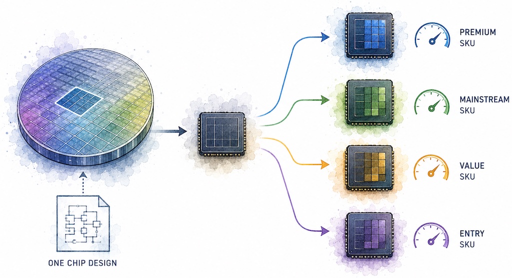
This approach is often called binning or soft SKUing. Features, cores, cache capacity or clock limits can be enabled or restricted through fuses, firmware or secure configuration, allowing multiple products to be created from one physical design. By matching each usable die to the best SKU it can support, manufacturers increase the number of saleable chips obtained from each wafer and improve the economics of production.
The first build remains the reference
The digital design does not lose its value when wafers arrive. Architecture models, RTL, test environments and layout databases remain essential for debugging, firmware development, security analysis, customer support and future chip generations.
A modern chip is therefore built digitally, built physically, measured against its models and often rebuilt in another stepping. The foundry creates the silicon, but the value of that silicon is determined by the decisions and evidence created before manufacturing.
What’s next?
Before first silicon exists, FPGA prototypes can already run real software and interact with sensors, networks and external systems. In the next article, we will examine how programmable hardware becomes the rehearsal stage for custom silicon.
Next article: FPGA - The Rehearsal Before Silicon
© 2026 Polski Krzem PSA